Topics for Student Research Papers, Bachelor- and Master's Theses at the Micro- and Nanotechnology of Electronic Systems
Handling and supervising may be done in English and naturally in German.
If you are interested or if you have further questions do not hesitate to meet us!
Contact: Prof. Dr.-Ing. D. Hohlfeld, Tel. 498-7205,Albert-Einstein-Str. 2, Ground floor "Seminargebäude", Room S 14.
Optical Waveguide Design
Data centers (e.g. Google, Microsoft and Amazon) and high-performance computing systems are currently integrating optical interconnects for on-board, board-to-board and rack-to-rack connections in order to satisfy the growing need for data transfer bandwidth and reduce power consumption.
This thesis or student project aims at the design of elementary building block of optical waveguides such as splitters, bends and crossings. CAD software (e.g. Autodesk AutoCAD) and simulation tools (e.g. COMSOL Multiphysics) will be used for layout generation and waveguide modelling. The results will be put into practice in a soon to be established manufacturing environment (project).
Further reading: Presentation by IBM on Optical Interconnects
Electron Beam Lithography for the Creation of Polymer-based Optical Waveguides
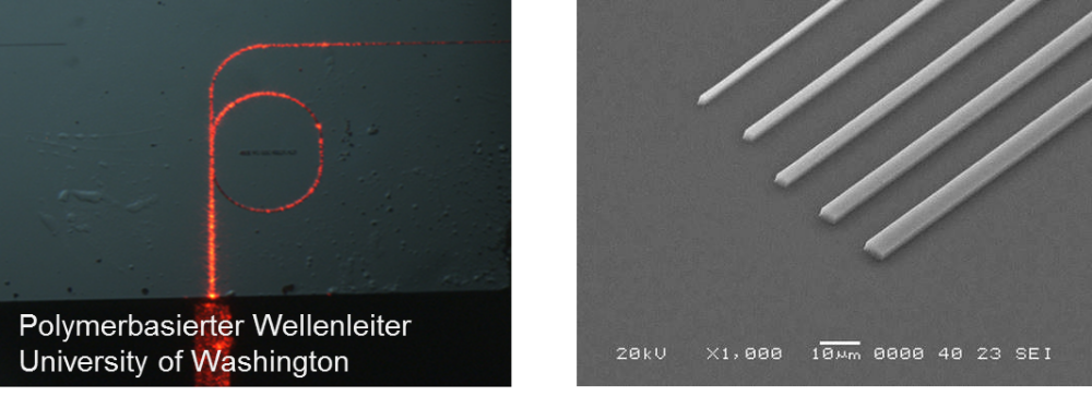
Unser Institut verfügt über ein Rasterelektronenmikroskop, bei dem der Elektronenstrahl nicht nur zur Bildgebung, sondern auch zur gezielten Belichtung spezieller Resiste eingesetzt werden kann.
Mittels dieser sogenannten Elektronenstrahllithografie können flächige Strukturen mit besonders hoher Auflösung hergestellt werden. Von besonderem Interesse sind hier z.B. Wellenleiter, optische Gitter oder sogar photonische Kristalle.
Im Rahmen dieser Masterarbeit werden mittels Elektronenstrahllithografie optische Wellenleiter hergestellt und charakterisiert (Einfluss der Prozessparameter auf z.B. Oberflächenqualität und Übertragungsverluste) und mit Wellenleitern aus konventioneller Fotolitografie verglichen.
Flyer: pdf
Weiterführende Informationen: Fundamentals of Electron Beam Exposure and Development, Elektronenstrahllithografie
Multiphysical Simulation of High Performance Computers
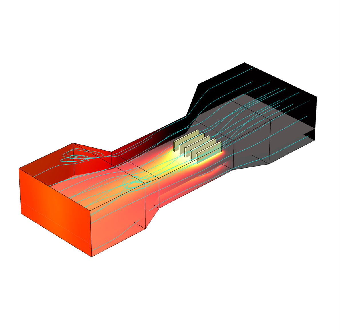
Die Leistungsfähigkeit moderner Hochleistungsrechner wird zunehmend durch die notwendige Entwärmung (Kühlung) limitiert. Aktuelle Systeme setzen hierzu komplexe Luftströmungen bzw. Wasserkühlung ein.
Im Rahmen dieser Thesis soll ein multiphysikalisches Simulationsmodell einer Server-Platine insbesondere um den konvektiven Kühlmechanismus erweitert und im Experiment verifiziert werden. Das Simulationsmodell beinhaltet derzeit thermo-mechanische Effekte. Eine Berechnung des Strömungsprofils und eine Berücksichtigung des konvektiven Wärmeübergangs sollen dieses Modell ergänzen.
Digital Light Processing (DLP) for PCB Lithography
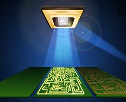
DLP is a programmable light steering technology. It is based on a digital micromirror array device (DMD) also used in projector systems. Here, it shall be used to expose photosensitive materials for resist pattern generation.
In the framework of this thesis an exposure system shall be designed and build, which allows to fabricate arbitrary patterns in a photosensitive resist. The project involves interfacing with the existing hardware and design of a suitable optical setup.
Further reading: Digital Light Processing, Digital Light Processing (TI), Digital Micromirror Array Device
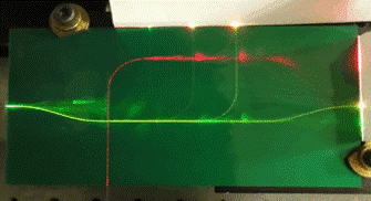
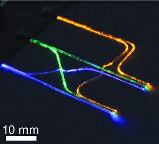
Camera based laser beam characterization for maskless lithography
In maskless lithography, optical waveguide structures are directly written onto electrical printed circuit boards coated with polymer by means of a focused UV laser beam (project). These optical waveguides play an important role in overcoming the bandwidth limitations posed by classical conductor paths made from copper.
This thesis will focus on the design and implementation of a beam profiler based on a standard CCD or CMOS chip able to characterize the laser beam quality (e.g. power distribution P(x,y,z), diameter, homogeneity, ellipticity, mininum spot size w0, quality factor M², etc.). Using this setup and dedicated ray tracing software, the exposure head may be optimized to generate the desired beam shape.
Further reading: Beam Profilers, Gaussian Beams
Optical waveguides for bio-medical sensing on PCB
Printed circuit boards (PCB) are highly integrated carriers for individual microchips for signal processing and sensing of parameters as e.g. motion, orientation, pressure, humidity. Realizing the sensing function itself with the PCB itself is a promising approach for increasing integration density.
The project will focus on the integration of optical waveguide based sensors for parameters for environmental and bio-medical parameters. Aspects such as waveguide fabrication, optical coupling and advanced sensing elements (optical resonators) provide potential for thesis specialization.
Contactless Power Transmission
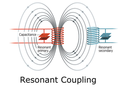
Berührungslose Energieübertragung, u.a. zum Aufladen von Mobilgeräten, (nach dem Qi oder Rezence Standard) hat sich im Alltag etabliert.
Diese Thesis adressiert Anwendungen mit höheren Leistungs- und Effizienzanforderungen, wie z.B. das Nachladen von Elektromobilen. Die Zielstellung dieser Thesis ist die Entwick-lung eines Systems zur berührungslosen Energieübertragung unter Verwendung einer resonanten magnetischen Kopplung. Dies kann entweder in Form eines Simulationsmodells oder als prototypischer Aufbau
erfolgen.
weiterführende Informationen: Drahtlose Energieübertragung, Qi standard, Rezence standard
System analysis and optimization of energy harvesting modules for wireless sensor networks
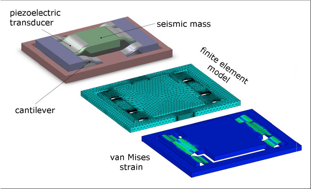
The work aims at design tools for accurate analysis of multiphysical systems. The thesis shall prove the feasibility to couple numerical models of energy harvesting microstructures with existing circuitry.
Current simulation techniques neglect the impact of circuit components on the MEMS behavior. The extensive time cost of models with large dimension renders their time transient simulation prohibitive. Model order reduction (project) will prove essential in order to enable truly system-level co-simulation of these systems at drastically reduced time cost. Furthermore, the established design flow shall be extended by system optimization.
Digital Light Processing (DLP) for Wavelength Control
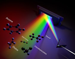
DLP is a programmable light steering technology. It is based on a digital micromirror array device (DMD) also used in projector systems. Here, it shall be used to manipulate optical spectra for applications in optical spectroscopy or optical networking.
This thesis project aims at the design and construction of an optical setup which incorporates a DMD for generation of arbitrary optical filter functions.
Further reading: Digital Light Processing, Digital Light Processing (TI), Digital Micromirror Array Device